Developing a wireless product can be a daunting task. There are many pitfalls, traps, and common mistakes people fall into during design and development. It is very common to save the implementation of the antenna for ‘last.’ The fact of the matter is that the antenna makes your product wireless. It is the most critical component that launches your signal into space. Often little consideration is given to the antenna location and how the object nearby can affect it. This can be devastating not only to a product’s performance, but also to schedule and cost.
Antenna Design and Environmental Factors
An antenna is a function of its environment. Whether it’s sitting on a desk, on a manufacturer’s development board, or in a product, all three scenarios result in different performance. Unlike most components in a design that can be dropped in with an expected effect on the circuit, an antenna is affected by everything around it. The radiated electromagnetic fields from an antenna interact with nearby materials, and can change its frequency of operation. The antenna must be placed in its final environment and impedance matched so that it operates in the desired frequency band. A poorly matched antenna can degrade your link budget by 10-30 dB and severely reduce range. All antennas, whether they are off-the-shelf or designed in a lab may require matching.
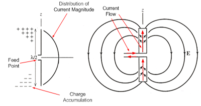
To understand why an antenna is affected by objects near it, how an antenna radiates must be reviewed. First, forget about what is happening to the antenna or what is nearby. What is important is the input impedance to the antenna. Examining the dipole in Figure 1, when a potential is applied to the antenna inputs there is opposite charge buildup on the ends. Essentially the dipole ends can be viewed as open circuits, with a high voltage and no current. Due to the charge buildup at either end of the dipole, current begins to flow. As you move from the end of the dipole inwards towards the feed point, the voltage falls and the current rises. At the feed point the current reaches its peak along with some now reduced voltage. The ratio between the voltage and current at the feed point is the input impedance to the antenna. This is the impedance that drives the antenna performance. Additionally, since there is current flow on the antenna electromagnetic fields are radiating.

Figure 1: Dipole Diagram
The antenna impedance acts as a load impedance for the transmission line that carries the signal to the antenna. The impedance of the antenna determines the voltage and current along the transmission line as well as their phase relationship. On the transmission line there is a Standing Wave Ratio (also known as VSWR). This ratio measures the amount of standing wave versus traveling wave. Roughly speaking, a VSWR = 1 means a pure traveling wave and a VSWR = ∞ means a pure standing wave. A very low VSWR is desirable because it indicates that most of the energy is being delivered to the antenna. A high VSWR means most of the energy is being reflect back onto the transmission line and is not being radiated. When the antenna is matched at the transmission line terminals, there is a low VSWR. Energy that is not delivered and instead reflected back at the antenna input can affect the RF circuitry, as it must be dissipated elsewhere.

Figure 2: Magnitude of Current and Voltage on Open Circuit Transmission Line
The antenna impedance changes with frequency because the current distribution is directly related to the wavelength. The current and voltage on the dipole form a sinusoidal distribution, so as the distance from the end of the dipole to the feed point varies by fractions of a wavelength, so does the impedance.

The antenna impedance must be kept as close to the impedance of the trace line feeding it as possible. In most systems there is a 50 Ohm trace going to the antenna. Since the antenna impedance changes with frequency, there is only a limited range that can be matched to the trace line for efficient power transfer. The process of matching your antenna over a range of frequencies to the trace line is referred to as ‘tuning’ or ‘matching’ the antenna. The quality of the match is characterized by VSWR, with Bandwidth referring to the range of frequencies that the antenna impedance is close to 50 Ohms for a given VSWR.
When the antenna is placed in an enclosure, the electromagnetic fields interact with the surrounding materials. As a result of this, the fields develop differently than they would in free space. This interaction ultimately changes the current distribution on the antenna, and consequently its impedance. This is why an antenna must be tuned in its final enclosure. The antenna impedance will shift depending on the proximity, electrical properties, and size of the surrounding materials. An antenna design can be ruined if it is not tuned properly during implementation.
RF Antenna Tuning
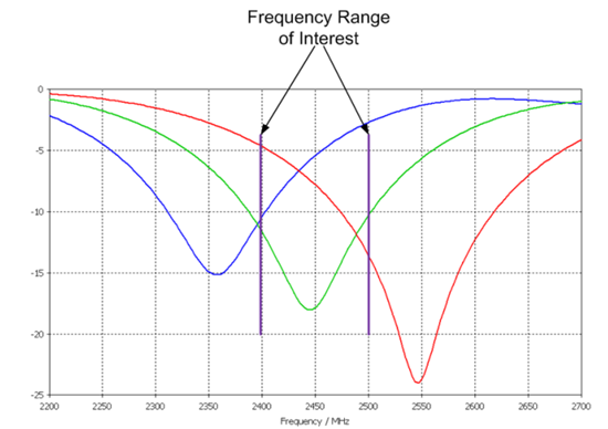
Antennas can be tuned one of two ways. Either by adjusting the dimensions or with a matching network typically consisting of discrete components. Typically changing physical dimensions is not an option, so a discrete network is placed just before the antenna input. The challenge with tuning an antenna is that its impedance is affected by nearby materials. If you tune the antenna to 2.4 GHz on your bench and then place it in an enclosure, the tuned frequency will shift. Figure 3 below demonstrates this effect. The red line is the antenna in free space, unmatched. The green line represents the same antenna now matched in free space. And the blue line is the final antenna response with it placed in the enclosure. Since the antenna was not tuned in the enclosure the impedance is not matched to the 50 Ohm PCB trace line over the frequency of interest. The antenna must be tuned in the enclosure to allow for the changes in impedance to be accounted for. This is true for all antennas, including chip and other pre-packaged antennas.

Figure 3: Frequency Shift of Antenna due to Mismatch
When deciding on a location for the antenna in your product, consider the following questions:
- What is the enclosure made out of?
- What will be near the antenna?
- Is there metal nearby?
- How will the device be used?
The material that your enclosure is made out of will dramatically affect how it tunes. Metal is extremely detrimental to antenna performance because it is conductive. Even paints with a very low percentage of metal in it will have a significant impact. Keep all metal objects (including PCBs) as far away from the antenna as possible. Electromagnetic fields create currents on metal objects, which turns them into small radiators. Not only does this hurt the match, but it will significantly reduce the gain pattern of the antenna. Additionally, the final use of the product must also be considered. Will the antenna be covered up by a hand? Will the product be mounted on a metal wall? All this can impact the tuning.
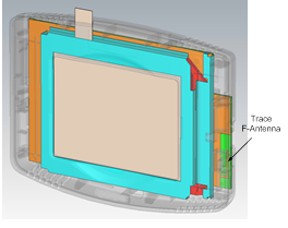
When it comes to tuning an antenna for its enclosure, there are many considerations. The process of tuning the antenna is difficult and time consuming. In many cases there are other PCBs, housing materials, batteries, display screens, metal brackets, and various other harmful objects nearby. All of these affect the tuning and must be present. The antenna location should be one of the first things considered when developing a new product; but it is often the last component to be finalized.

Figure 4: Antenna Integrated Into Product, Designed in CST Microwave Studio at Ezurio (formerly Laird Connectivity)
The most effective method to anticipate antenna tuning and radiation problems is to use simulation software to evaluate and predict the effects of an enclosure. An antenna designer must identify the materials in the product, define their electrical properties, and understand how the antenna will interact with them. A well designed and simulated antenna will usually require no matching network; however it will only be tuned correctly for the exact product it was designed for.
Antenna Selection and Placement
Antenna selection and placement can be a difficult task, and the challenges of implementing the antenna are not over once it’s placed on the board. As previously discussed earlier in the paper, the enclosure affects the antenna match. The process of matching an antenna can be a very complicated process. Not only is an in-depth knowledge of RF principles and components needed, but proper technique and understanding of the antenna properties is required. Any error introduced into the measurement while matching the antenna will ultimately reduce the effectiveness of the antenna and its performance. For this reason, as much care should be taken in the setup of your measurements as the actual matching process itself.
The most important factors in antenna tuning are proper connection to the PCB, calibration and port extension of the network analyzer, and knowledge of the antenna to ground plane relationship. These three factors must be taken into account when attempting to tune an antenna for an enclosure, and will be covered in this paper. Tuning an antenna is not as easy as simply connecting it to a network analyzer and chasing the impedance around the smith chart. Without doing the little steps right, it is easy to introduce error into the measurement and improperly match the antenna.
Before matching can begin, a proper connection must be established to the PCB. There are usually two methods for connecting to the PCB to match an antenna. The first is using a U.FL connector. This involves finding an area big enough to place the connector down and an area that allows for good grounding. It is often difficult to find enough room near the antenna trace for this method; additionally care must be taken to make sure you don’t introduce additional parasitic effects. The U.FL is typically only effective for tuning if the PCB was designed with specific component pads for placement of the U.FL. The second, more common method is to strip a thin coaxial cable and solder it directly to the trace line. This requires less space on the PCB and is more flexible than placing a U.FL on the board.
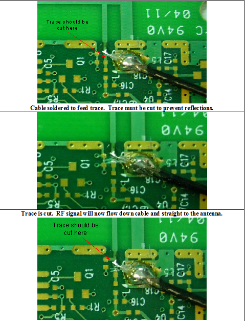
When soldering a coaxial cable to the PCB, the inner conductor must be soldered to the beginning of the trace and the outer shield well soldered to ground. Occasionally, it is not possible to solder to the beginning of a trace (see Figure 5). This will give an inaccurate measurement of the antenna’s impedance. The RF signal propagates down both ends of the trace at the same time. The signal will reach the end of the stub, reflect back, and interfere at the solder point to give false impedance readings. To eliminate this problem, the trace behind the solder point has been cut. The RF signal will now propagate down the cable and only to the antenna. Similarly, as shown in the third picture of Figure 5, make sure there are no extra lengths of trace line after solder point as well. This will result in the same reflections problem.

Figure 5: Soldering a Cable to an Antenna Feed Trace
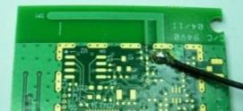
Small PCBs can be particularly difficult for tuning because of their ground plane size. This is a common a problem with chip antennas because they are placed on very small boards. With a small ground plane, the outer conductor of the coaxial cable can act as the antenna ground. This causes currents to flow on the outer conductor of the cable. As a result, the cable actually becomes part of the antenna and radiates. An easy way to test for this is by touching the coaxial cable, if the S11 measurement on the network analyzer shifts significantly, this indicates a problem. This can be rectified by making sure the cable is well connected to ground. If this still does not solve the issue, other methods including adding a ferrite or routing the coaxial cable different may help.

Figure 6: Trace F Antenna
After the cable has been properly attached to the antenna feed trace, the network analyzer needs to be calibrated. The antenna in Figures 5 and 6 is a trace F. This type is designed to be tuned without matching components. The F has been intentionally created too long, and hence tunes too low in frequency. The advantage to doing this is that the engineer can slowly trim the end of the antenna and increase the resonant frequency. This technique can be used to tune a trace antenna in its final enclosure. Table 1 below documents the trimming and tuning of the F antenna above. The desired frequency band is 2.4 GHz. This represents the most basic form of tuning an antenna. The dimensions are being physically altered, which is changing the impedance of the antenna, and consequently the load seen by the transmission line delivering the RF signal.
This trace F antenna example was designed at Ezurio. The overall dimensions for the feed width, trace width, height, and feed location were determined through simulation. The final step of tuning by trimming the overall length can be done on a bench, but optimization of the antenna dimensions for bandwidth and Return Loss should be done by an experienced antenna designer.
Figure 7: Trace Antenna Tuning
While the previous example relied on looking at an S11 measurement on a network analyzer, most commonly an engineer will have to match an antenna via a discrete network of inductors and capacitors. Antennas that are purchased ‘off the shelf’ will require matching, the antenna dimensions cannot be altered as with the F example above. In order to match an antenna with components, an in depth knowledge of the Smith chart is needed to properly determine the matching network.
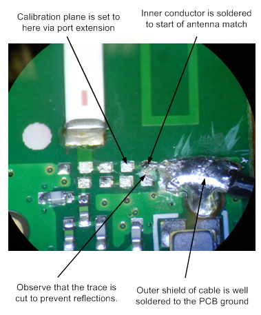
When employing the use of matching components, the coaxial cable for measurement should be soldered on before the matching network. In the F antenna example, since it was being tuned without components, the coaxial cable had to be a directly connected to the feed. As shown below in Figure 8 and Figure 9, the cable is now placed before the matching network. In addition to properly placing the cable, the port extension feature of the network analyzer is needed. Since the Smith Chart will be used to determine the impedance of the antenna, the reference plane for the measurement must be correctly set. Since the cable is soldered directly to the board, you cannot calibrate to the end of it. A port extension must be applied to account for the phase change of the additional length of cable not included in the calibration. This will essentially move the calibration plane past the cable and to the end of the trace. If this is not done, impedance measurements on the Smith Chart will not be correct.

Figure 8: View of Matching Pads and Cable Under a Microscope
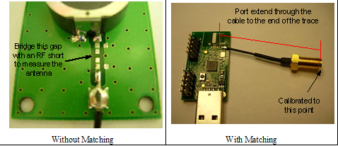
With the port extension properly set, the antenna impedance must be measured so that a matching network can now be designed. An RF short should be used to bridge the gap in the trace lines. However, whatever component is used to bridge the gap will inherently add some of its own capacitance or inductance to the measurement. At frequencies under 1 GHz, a 0 Ohm jumper is may be used as a short. However, at higher frequencies, the 0 Ohm jumper becomes inductive and will introduce error into the measurement. This is especially true for anything above 1 GHz. The best thing to use to bridge the gap is a capacitor that is resonant near your frequency of operation. This will eliminate most of its inductive or capacitive qualities. For example, an 8.2pF Murata GRM 0402 capacitor is resonant at approximately 2.4 GHz. While it’s not a perfect RF short, it is much better than a 0 Ohm jumper or a glob of solder. Both of the later alternatives will be inductive at higher frequencies. Also, the resonant frequency of the capacitor will vary depending on the manufacturer. A 10pF Johanson 0402 L-Series capacitor is a good RF short at 2.4 GHz. Make sure to have a thorough understanding of the components being used.

Figure 9: Puck Antenna Board
Another key component that significantly affects the tuning and also radiated performance of an antenna is the ground plane. Many antennas, particularly traces and chips, are dependent on the shape and size of the PC B ground plane. The chip (or trace) is only half of the antenna, the other half is the ground plane. Recalling the dipole diagram and current distribution from earlier in the paper, there is positive and negative charge buildup on the antenna. This buildup of charge is ultimately what causes current flow. In a similar fashion, charge builds up on the trace antenna and on its corresponding ground plane. There is current flow on the antenna due to this charge, but since the ground plane is now partially responsible for the charge buildup it will also directly affects the current distribution and ultimately the impedance and radiation of the antenna.
Manufacturers for chip antennas commonly give recommended matching circuits, but these are only valid if the PCB is the same size as the one the manufacturer tested with. Additionally, testing at the manufacturer would have been done in free space, using the chip antenna within an enclosure forces it to be re-tuned. Essentially, the recommended matching circuit is not usable for most implementations and the antenna must be re-tuned. Additionally, the orientation of the chip antenna with respect to the ground plane will affect tuning and performance. The datasheet for the chip antenna will depict an orientation and keep out area. This is should followed as closely as possible!
The key to successfully matching an antenna is maintaining accuracy in the measurement. Good grounding of the coaxial shield, proper solder location on the feed line, and knowledge of your component are all very important. Small inaccuracies can easily result in an engineer designing the wrong matching network for an antenna. This paper has covered some common mistakes, but overall a good understanding of RF principles is the best tool for matching an antenna.
 Laird Connectivity is now Ezurio