 Laird Connectivity is now Ezurio
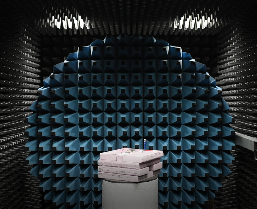
EMC Testing Defines Your Product's Future - Here's How
Published on February 20, 2020
Understanding the Problem – Interference is Everywhere
No matter what your device does or where it operates, if it’s an electronic device it is capable of both creating and receiving unwanted electromagnetic behavior. Wherever an electrical current moves, there is always the creation of an unintended magnetic signal – it’s a necessary byproduct of electronic design, and it’s impossible to fully silence.
However, in the worst cases, electromagnetic interference is not a nuisance, it’s genuinely destructive to the integrity of your devices and devices nearby. It can be narrowband in scope and only affect a small frequency range, or can be broadband in scope and scatter signal across a wide array of frequencies. For this reason, regulatory bodies around the globe require manufacturers limit the amount and type of interference your device may generate, and have well-defined limits and testing procedures to be sure your device performs as expected.
It’s important to understand the potentially destructive impacts of electromagnetic interference, as well as to understand the means and measurements that determine compliance. But more than this, it’s important to understand just how early these problems can crop up – and how your test plan determines the success of your product’s development and its future in the market.
What is EMC Testing?
Electromagnetic compliance (EMC) testing is the process of identifying sources of electromagnetic interference (EMI) in your design, for the purpose of reducing interference radiating from your device. By scanning your device while it’s in operation, a test house can determine a full 360-degree assessment of the radiation your device gives off, and to help isolate circuits and components which may be responsible for generating unacceptable levels of unintended radiation.
The testing is conducted in an anechoic antenna chamber, the purpose of which is to help measure just the radiation coming directly from the device, and to dampen secondary reflections off the surfaces of the chamber itself. The device is either rotated on a podium and measured by a stationary antenna, or is kept stationary while a revolving arm takes measurements at multiple positions. In the case of wireless devices, they are controlled by software to test their radiative performance at various configurations and power levels. The goal is to obtain a complete picture of the RF characteristics of the device in all its operating conditions, to fully understand its emissions in every scenario.
With this picture fully realized, it’s possible to look for design faults and interferers which compromise the system or can compromise other collocated systems.
There is also the separate matter of EMC immunity testing, which is something like the opposite of EMI testing. Where EMI testing looks to identify the sources of interference radiating from your product, EMI testing attempts to demonstrate your device’s resistance to interference from other devices. This is useful for products designed for mission-critical scenarios or products that are integrated in highly noisy RF environments. Instrumentation on airplanes is an example, where instruments must resist nearby interference and operate under difficult conditions.
What causes EMI?
As mentioned, EMI can be generated by nearly any electrical activity throughout a circuit, as electrical current by necessity generates a magnetic field. However, some components are more likely to generate EMI, or to generate more EMI than others. In our white paper on RF design considerations, we’ve outlined how small changes in hardware design can have a major impact on performance. Those impacts are much more exaggerated in high-frequency RF design than they may be in other applications
Resistors, capacitors, and inductors tend to produce negligible EMI effects in low-frequency utilization, but in high-frequency RF applications they’re more likely to generate parasitic effects that can degrade or destroy signal.
Sometimes mitigating those effects may simply mean selecting different components. For example, where an 0805 resistor may generate an unacceptable amount of noise at high frequencies, smaller resistors may have significantly better performance. This is the sort of unexpected behavior that only EMC testing can identify and address.
Something as simple as material density can create a significant source of EMI as well. When a wave encounters an interface between two materials of different densities, the reaction is that some of the wave is reflected backwards. It’s sort of like a bottleneck: on encountering resistance, signal is slowed and pressure reflected back in the opposite reaction. And, like the EMI generated in ICs, only testing and measurement can identify these problems where they may otherwise remain invisible.
Why is EMC Testing so Important?
Knowing everything you can about your product’s radiated performance and its sources of interference is critical for many reasons. Some of those reasons are local just to your device and its performance, but at a higher level, it’s important for achieving regulatory approval and deploying your device into various regulatory regions.
At the most local level, unintended radiation can be a symptom of a greater problem within your design. High levels of interference can be indicators of poor manufacturing or a faulty design which can have serious impacts on RF performance for wireless radios.
The results of EMC testing can give you a route forward, especially early in a product design, on how to ensure regulatory compliance down the line. Changes to a hardware design are much costlier and more difficult later in the product design cycle, and so insights into faulty design at the early stage are highly valuable. We recommend pre-scans throughout the design process for this reason, as detailed in our white paper on FCC pre-scans. Discovering problems early can make it much easier to keep your product on schedule and within budget, and EMC testing is the only way to be certain that your product is performing as it does on paper.
When to EMC Test Your Product
Generally speaking, if you’re considering whether it’s time to begin scans on your product, it’s already time. As soon as you have early hardware, you can be prepared to iterate by analyzing that design for its unintended radiation characteristics.
If your product is of a wireless nature, such as Bluetooth, Wi-Fi, Cellular or other wireless standards, it’s even more critical to get early scans to get a clear picture of your design. While EMI can interfere with many board-level circuits and components, it’s especially detrimental to a data path like a wireless link. Where EMI can degrade performance or introduce noise in board-level components, it can degrade or even fully destroy a wireless link. It’s critical to know very early on which elements of your design are causing problems, and to adjust them early in the process before your design starts to get locked in.
This means multiple tests across the design phase from a qualified test house, who have the tools and expertise to generate that data and make helpful recommendations about the vulnerabilities in your design. Ezurio's (formerly Laird Connectivity) in-house EMC testing experts can test your product (even very large products, in our 5M anechoic chamber) early and often, and can help bring your product from its infancy into full worldwide regulatory compliance.
Learn more about how Ezurio's EMC Testing services can bring your product safely to market.